Electronics and Semiconductor Manufacturing Industry

haldilal

लड़ते लड़ते जीना है, लड़ते लड़ते मरना है.
Administrator
Joined
Jun 27, 2024
Messages
1,006
Likes
3,124
Will discuss all about the Indian Semi Conductor developments on this thread.

 
Last edited:
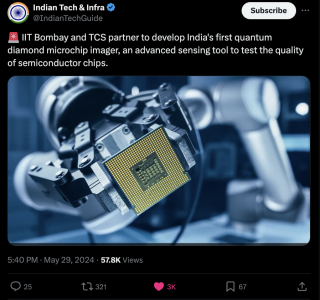
Synopsys TATA collaboration.


1719998387418.png
1719998403388.png


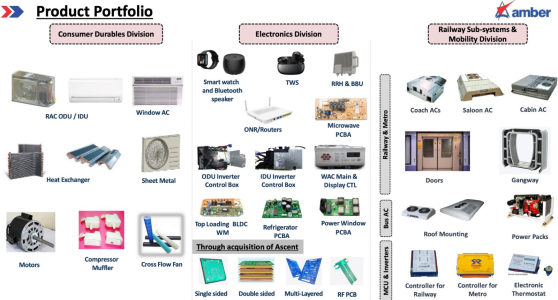
At 2000crores, this seems like a sufficiently big facility with multiple SMT lines and advanced machinery. If this gets built out, it might be one of the few factories in India that can directly compete with Shenzhen on costs for PCBs. Wages are much lower here which will offset any higher electricity cost.

1719998444059.png


Last edited:


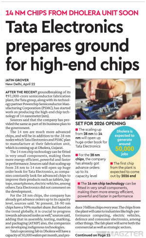
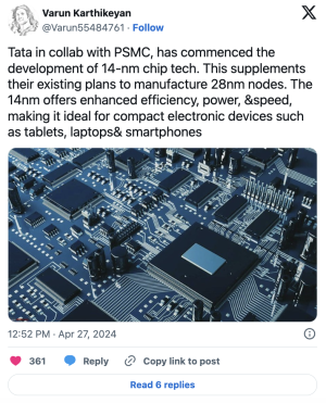
TEPL will go down to 14nm chips
1719998510318.png


As per this article from this year, out of the 13 OEMs listed , 3 are Indian & 2 figure in the top 10 list by way of percentage of global market share.

That's some achievement & it completely evaded the radar.


1719998577376.png
 
1719998809016.png


New PLI
1719998923291.png


1719998952202.png


Tata begins export of chip samples


1719999189319.png


According to officials, if the government decides to take SCL’s capacity to 20,000 wafers, the planned investment would be around Rs 20,000 crore ($2.5 bn).
 
1719999608967.png


India will soon start making equipment for semiconductor manufacturing, Union telecom and IT minister Ashwini Vaishnaw said on Saturday.
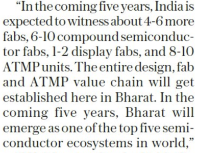
"The entire semiconductor ecosystem of fabs, ATMP units, chemicals, gases, substrate, consumables and equipment for semiconductor manufacturing will be made in India," he said.
He was speaking at the inauguration of American chip equipment supplier Applied Materials' India Validation Centre in Bengaluru which was set up at a cost of $20 million.
Such labs are present in the US, Singapore, China and Korea. The India Validation Centre will have a workforce of 500 people.
The company last year announced that it will set up an engineering centre in Bengaluru with a total investment of $400 million over four years to develop and commercialise technologies for semiconductor manufacturing equipment.
Vaishnaw said that the components that were earlier imported from Japan, Korea and Taiwan are being made by the company here now.
"Today, all the four agreements made during the Prime Minister's state visit to the US have been materialised," Vaishnaw said.
The construction of Micron's ATMP has commenced. In addition, LAM Research's proposal to deliver a virtual nano fabrication environment through its Semiverse Solutions to train semiconductor engineers in India has also started.
"The first training course in the Indian Institute of Science has started with 35 students," the minister said. The third agreement was in relation to a centre of Applied Materials to be set up in India, he said. "This has also fructified with a centre of the company being set up here," he said.
A design centre of Advanced Micro Devices (AMD) was also to be set up in India. "A few months back, I inaugurated the design centre of AMD in Bengaluru," Vaishnaw said.
A first for 300 mm wafer processing
Sonny Kunnakkat, managing director, Advanced Manufacturing Technology, Worldwide Operations, Applied Materials, told ET that this is the first private facility in India that will process 300 mm wafers.
So far, 200 mm wafers have been processed in India.
"We used to have a 300 mm processing facility in the Indian Institute of Technology but that was academic. This is a commercial one. We will do our own development work. The wafers that we make are not sold as we are an equipment company and not a chip company. Our equipment here will go to our customers to make their chips," Kunnakkat said.
The change rate of the equipment is very fast, he said. Equipment and components must be continuously developed with evolving customer challenges. "That is the kind of development that will be done here," he said.


1719999819294.png


'India will soon make equipment for semiconductor manufacturing'
Synopsis
Union telecom and IT minister Ashwini Vaishnaw announced that India will start manufacturing equipment for semiconductor manufacturing. Applied Materials' India Validation Centre, an investment of $20 million, will have a workforce of 500 people and is the first private facility in India for processing 300 mm wafers.
India will soon start making equipment for semiconductor manufacturing, Union telecom and IT minister Ashwini Vaishnaw said on Saturday.
"The entire semiconductor ecosystem of fabs, ATMP units, chemicals, gases, substrate, consumables and equipment for semiconductor manufacturing will be made in India," he said.
He was speaking at the inauguration of American chip equipment supplier Applied Materials' India Validation Centre in Bengaluru which was set up at a cost of $20 million.
Such labs are present in the US, Singapore, China and Korea. The India Validation Centre will have a workforce of 500 people.
The company last year announced that it will set up an engineering centre in Bengaluru with a total investment of $400 million over four years to develop and commercialise technologies for semiconductor manufacturing equipment.
Vaishnaw said that the components that were earlier imported from Japan, Korea and Taiwan are being made by the company here now.
"Today, all the four agreements made during the Prime Minister's state visit to the US have been materialised," Vaishnaw said.
The construction of Micron's ATMP has commenced. In addition, LAM Research's proposal to deliver a virtual nano fabrication environment through its Semiverse Solutions to train semiconductor engineers in India has also started.
"The first training course in the Indian Institute of Science has started with 35 students," the minister said. The third agreement was in relation to a centre of Applied Materials to be set up in India, he said. "This has also fructified with a centre of the company being set up here," he said.
A design centre of Advanced Micro Devices (AMD) was also to be set up in India. "A few months back, I inaugurated the design centre of AMD in Bengaluru," Vaishnaw said.
A first for 300 mm wafer processing
Sonny Kunnakkat, managing director, Advanced Manufacturing Technology, Worldwide Operations, Applied Materials, told ET that this is the first private facility in India that will process 300 mm wafers.
So far, 200 mm wafers have been processed in India.
"We used to have a 300 mm processing facility in the Indian Institute of Technology but that was academic. This is a commercial one. We will do our own development work. The wafers that we make are not sold as we are an equipment company and not a chip company. Our equipment here will go to our customers to make their chips," Kunnakkat said.
The change rate of the equipment is very fast, he said. Equipment and components must be continuously developed with evolving customer challenges. "That is the kind of development that will be done here," he said.


Polymatech invests US$ 1 Billion in Semiconductor chips manufacturing​


Sahasra Semiconductors starts production at its Bhiwadi unit
Mumbai: This Indian manufacturer has become the first company to produce memory chips in India, even before Micron. Rajasthan-based Sahasra Semiconductors has started production at its semiconductor assembly, test and packaging unit in Bhiwadi district this month and made its first shipment to e-commerce platforms.
 
Just over a year ago we were all on hopium for 1-2 fabs and seething over the foxconn vedanta failure . Recent developments are absolutely wild .
 

Latest Replies

Featured Content

Trending Threads

Donate via Bitcoin - bc1qpc3h2l430vlfflc8w02t7qlkvltagt2y4k9dc2

qrcode
Back
Top