Interesting. The conventional solar panels are made of Silicon and they top out at 20% efficiency which drops gradually over a period of time. The perovskite solar panels are still in research phase. They do deliver higher efficiencies compared to silicon, but they degrade faster than silicon. Here in this case they are using both. Top layer is perovskite and the layer underneath is silicon. If they can somehow prevent the degradation of perovskite layer then they have a goldmine in their hands.
To put things in perspective, let me elaborate on this. There are 2 types of Solar panels widely in use.
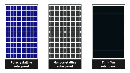
1) One is Monocrystalline and the other Polycrystalline. It is easy to spot which type of solar panel by a naked eye. If you see a black solar panel then it is monocrystalline. This is made from single silicon crystal which allows easy movement of electrons inside the cell resulting in high efficiency. They generate decent amount of electricity even during cloudy days. Ofcourse, monocrystalline panels are expensive.
2) Second one is Polycrystalline. This one is blue in color. This is made from multiple silicon crystals allowing for lesser mobility of electronics resulting in less efficiency. This panels are cheaper.
View attachment 43578
In India it takes 25 square km of land for installation of 1 GW of Solar. Most of them use Polycystalline panels for cost reasons. Some use a mix of both. For 1,000 sq.kms we can have 40 GW solar installation. If we can commercialize the solar panel with 29% efficiency, then we would need 20 sq.km of land which would make a big difference when we scale. In the same 1,000 sq.kms land area we can now have 50 GW solar installation. That makes a huge difference.


